
Micron is reportedly working on a new kind of near-GPU NAND flash designed to sit much closer to a graphics processor than storage traditionally does, according to industry reporting on the company’s research direction. Rather than parking data in a drive several steps removed from the GPU behind a chain of controllers and protocols, this flash would live right on the GPU package or its circuit board, acting as a fast buffer between memory and mass storage.
The idea responds to a very specific problem in artificial intelligence hardware: running enormous large language models without needing an ever-growing stack of expensive memory chips. If it pans out, near-GPU NAND flash could change how AI accelerators are built over the next few product generations.
Table of Contents
What Near-GPU NAND Flash Actually Is
Current GPU memory hierarchies are built around speed above almost everything else. High Bandwidth Memory (HBM) sits directly next to the compute die, offering enormous bandwidth but at a high cost per gigabyte. Regular system storage, by contrast, is cheap and dense but sits far away, reached through several layers of software and hardware that add latency no AI accelerator wants during inference.
Near-GPU NAND flash is pitched as the middle layer between those two extremes. It would use NAND cells with lower density than standard TLC or QLC flash found in consumer SSDs, trading some capacity for much faster read times, better I/O, and higher endurance. The goal is not to replace HBM or DRAM, but to give GPUs a large, moderately fast pool, potentially hundreds of gigabytes, that sits right on the package rather than across a cable or bus.
Why Big AI Models Need a New Memory Tier
Large language models keep growing, and the memory needed to run them scales with parameter count. When a model’s data exceeds available GPU memory, systems either need more GPUs to spread the load or accept a performance hit shuttling data from slower storage. Both options are costly, whether measured in hardware or in wasted compute cycles waiting for data to arrive.
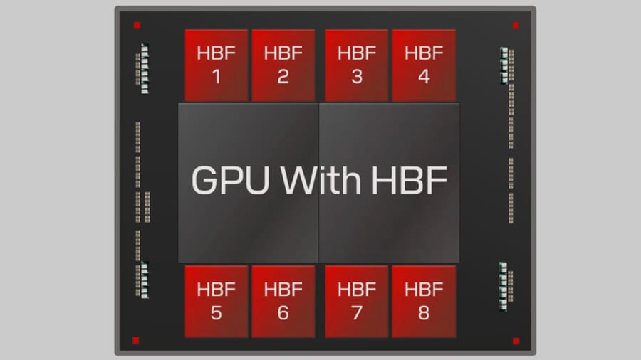
Near-GPU NAND flash aims to soften that constraint. By giving each GPU access to a large, fast local pool that behaves more like memory than a traditional drive, inference workloads could draw on far more effective capacity without demanding a proportional increase in HBM or DRAM. Because inference workloads for massive models are often bound by memory capacity rather than raw compute throughput, this middle tier could let a data centre run bigger models on fewer GPUs than would otherwise be required, easing pressure on already constrained AI hardware supply.
How It Stacks Up Against HBM and Rival Concepts
Micron is not alone in exploring this space. SK hynix and SanDisk have both discussed a related concept known as High Bandwidth Flash (HBF), which similarly aims to place NAND-based memory closer to compute for AI inference tasks. The broad direction across the memory industry looks similar: keep HBM and DRAM for the fastest, most latency-sensitive work, and introduce a new flash-based tier underneath for bulk data that still needs to be fast, just not HBM-fast.
| Memory tier | Typical role | Relative speed | Relative cost per gigabyte |
|---|---|---|---|
| HBM / GDDR7 / LPDDR6 | Primary GPU working memory | Highest | Highest |
| Near-GPU NAND flash (proposed) | Fast buffer for large model data | Moderate to high | Moderate |
| Standard TLC/QLC SSD storage | Bulk system storage | Lowest of the three | Lowest |
The appeal is straightforward. Near-GPU NAND flash would cost noticeably less than adding more HBM or DRAM, while still being sized to whatever a given system actually needs, rather than forcing buyers into fixed, expensive memory configurations.
What It Could Mean for the Industry
None of this is close to a shipping product yet. Micron’s exploration of near-GPU NAND flash remains at the research stage, and there is no confirmed timeline for when, or whether, it will reach commercial GPUs or AI accelerators. Still, the direction reflects a broader shift in how memory and storage makers are approaching the AI boom, treating the gap between fast memory and slow storage as a genuine design opportunity rather than an unavoidable trade-off.
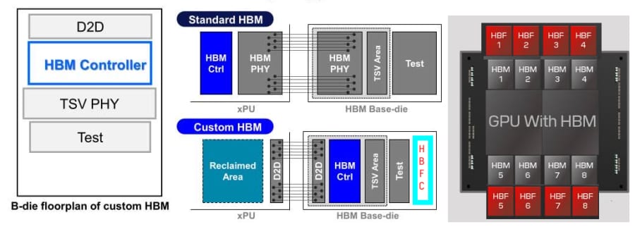
For data centre operators and AI developers, a workable near-GPU NAND flash tier could eventually mean lower hardware costs per deployed model and less reliance on scarce, expensive HBM supply. It also puts more competitive pressure on rivals working on SanDisk’s high bandwidth flash work and similar efforts, since whichever company gets a viable product to market first stands to gain significant traction with AI hardware builders. Given how central NAND flash makers racing to expand capacity have become to the wider memory market, this kind of specialised, high-endurance flash could open an entirely new revenue category for Micron and its competitors, well beyond conventional SSDs.
It also echoes trends already playing out in enterprise storage, where enterprise all-flash storage arrays have pushed flash into roles once reserved for spinning disks. Applying that same logic directly to GPU packages, rather than network-attached storage boxes, is a natural next step as AI workloads keep pushing the limits of existing hardware. Anyone tracking how GPU memory shapes performance in consumer graphics cards will recognise the same underlying tension at a much larger scale in data centre AI accelerators, where memory capacity, not raw compute, increasingly decides what a system can actually run.
For now, near-GPU NAND flash remains a concept rather than a confirmed product from Micron. Whether it reaches real silicon will depend on how well the company can balance endurance, cost, and speed at the scale modern AI training and inference demand.